The Hidden Mechanism Behind Semiconductor Fab
Here is the weird part: a semiconductor fab is not really making a chip. It is preventing failure. One wafer must hold billions of switches, and one dust speck or tiny misalignment can wreck huge regions.
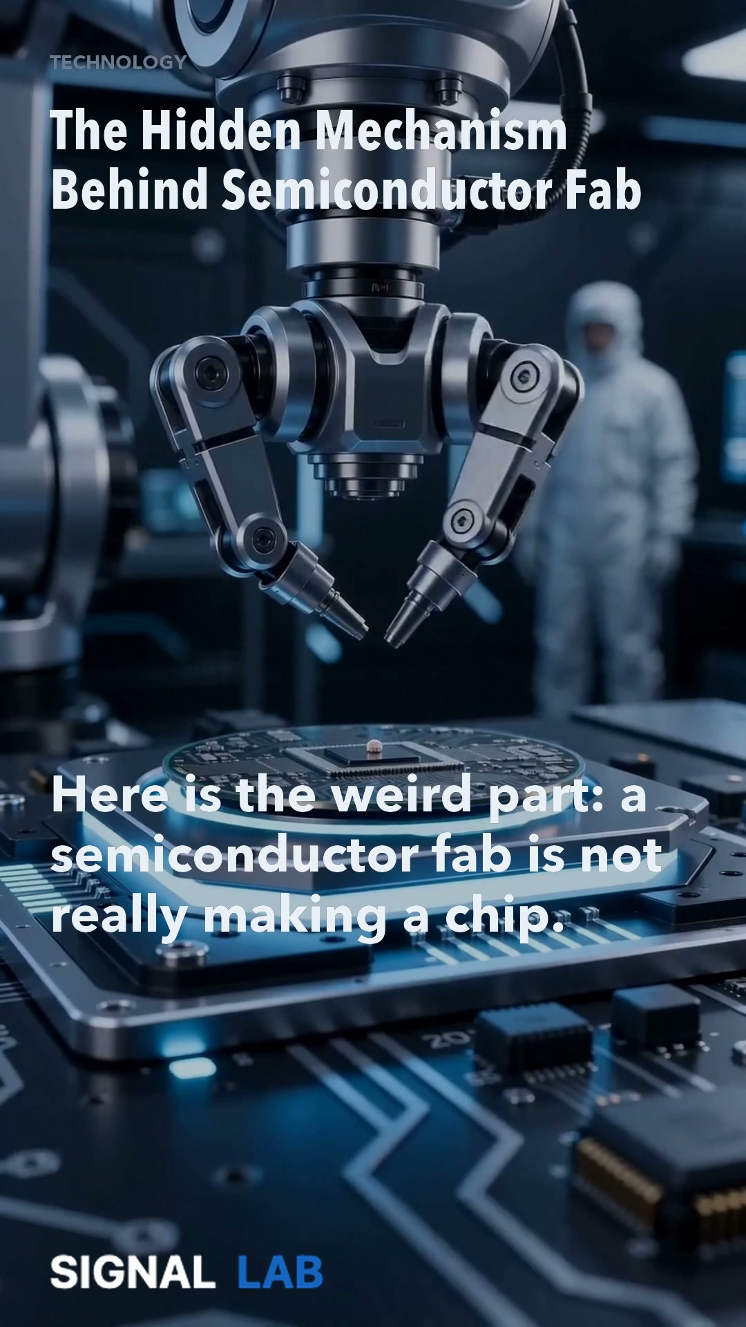
Here is the weird part: a semiconductor fab is not really making a chip. It is preventing failure. One wafer must hold billions of switches, and one dust speck or tiny misalignment can wreck huge regions.
That is why the base wafer matters so much. Silicon is purified, formed, sliced, and polished until it is almost perfectly flat, because every transistor, contact, and wire built later inherits that starting surface.
Then the fab writes with light. A liquid coating called photoresist spreads into a thin film, and extreme ultraviolet flashes pattern it. The trick is shorter wavelength light, guided by ultra-precise mirrors, so edges stay sharp enough to matter.
After that, chemistry and ion beams carve, tune, and repeat the pattern layer by layer, then metal wiring connects it all. So the hidden mechanism is not one miracle machine. It is controlled repetition, stacked until polished silicon becomes computation.
Key facts
- And AI response depends on switches so small they are hard to picture.
- And AI response depends on switches.
- Small they are hard to picture.
- A modern chip packs billions of transistors onto one silicon wafer.
- So the real question is not what a chip does.
Why it matters
But how any factory can build structures that small. Without drifting out of control.
The Signal Brief
One sourced idea worth your attention, in your inbox. No noise.